uPDM4 Datasheet
The Micro PDM4 is a smart 4 channel power distribution module designed to replace mechanical relays and fuses in aftermarket automotive electrical circuits. Each of the 4 outputs can supply up to 15 amps continuous load current. Each output can be triggered by switch inputs or CAN messages. Outputs feature PWM soft start capabilities.
In applications where installers may need to add a small number of power circuits but don’t require the size, cost or complexity of a full scale PDM. The Micro PDM4 is perfect for coupling with new engine harness builds or when adding a wide range of auxiliary circuits to a vehicle.
The uPDM4 is constructed from AEC-Q100 Automotive Grade components, ensuring its reliability in harsh environments.
Overview
- 4x Outputs, 15A Nominal, 24A Max
- 5x Analogue/Digital Inputs
- CAN 2.0B / FD Communications
- Over current Protection
- Over temperature Protection
- Short Circuit Protection
- Automotive Grade Device
Applications
- Resistive, Inductive and Capacitive Loads
- EFI relay
- ECU, DBW, Coil, Injector supplies
- Fuel pumps
- Water pumps
- Thermo fans
- Vehicle lighting
Wiring Pinout
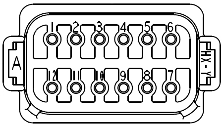
| Pin | Name | Description |
|---|---|---|
| 1 | OUT1 | 15A High side load output 1. PWM up to 200Hz. Soft start capable. (1) |
| 2 | OUT2 | 15A High side load output 2. PWM up to 200Hz. Soft start capable. (1) |
| 3 | OUT3 | 15A High side load output 3. PWM up to 200Hz. Soft start capable. (2) |
| 4 | OUT4 | 15A High side load output 4. PWM up to 200Hz. Soft start capable. (2) |
| 5 | IN5 | Analog/Switch/Frequency input 5. 0-20V. Configurable 4K7 pull up to 5V0. (3) |
| 6 | CANH | CAN High. |
| 7 | CANL | CAN Low. |
| 8 | GND | Chassis ground. |
| 9 | IN4 | Analog/Switch/Frequency Input 4. 0-20V. Configurable 4K7 pull up to 5V0. (4) |
| 10 | IN3 | Analog/Switch/Frequency Input 3. 0-20V. Configurable 4K7 pull up to 5V0. (4) |
| 11 | IN2 | Analog/Switch/Frequency Input 2. 0-20V. Configurable 4K7 pull up to 5V0. (4) |
| 12 | IN1 | Analog/Switch/Frequency Input 1. 0-20V. Configurable 4K7 pull up to 5V0. (4) |
| M6 Stud | BATT | Battery positive supply. |
- Rev 1 Hardware (Serial# < 2000) Only: Pins OUT1 & OUT2 share a common frequency register. The lowest of the two requested frequencies will drive the two outputs. Duty cycles remain independent to all channels.
- All Hardware Versions: Pins OUT3 & OUT4 share a common frequency register. The lowest of the two requested frequencies will drive the two outputs. Duty cycles remain independent to all channels.
- Rev 1 Hardware (Serial# < 2000) Only: No configurable pullup on IN5, fixed 10K pull down to GND.
- Rev 1 Hardware (Serial# < 2000) Only: No configurable pullup on IN1-4, fixed 10K pull up to GND. No voltage measurement, digital inputs only.
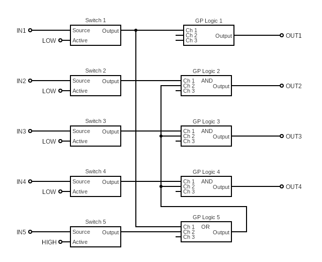
Default Configuration
By default, General Purpose Logic 1-4 are configured to drive OUT1-4 respectively.
IN1-5 drive Switch 1-5 respectively.
General Purpose Logic 1-4 are fed by Switch 1-4 respectively.
General Purpose Logic 5 is fed by Switch 1 OR Switch 5.
General Purpose Logic 2-4 require either Switch 1 or Switch 5 to be in some form of active state to enable.
This configuration makes OUT1 always switchable and acts like a master enable for the remaining OUTn pins.
All outputs are switchable if IN5 is high. This acts like a master ignition switch input.
This functionality has been chosen because some ECU’s which may be driving the INn pins default to a low state when they are switched off. This can result in the output channels being enabled in error. OUT1 being always switchable makes it useful for EFI main relay duties.
All outputs can be controlled by CAN at any time, regardless of their driving function’s.
| Pin | Config | Fuse Current | Retries | Retry Delay |
|---|---|---|---|---|
| OUT1 | GP Logic 1: IN1 Active | 12.0 Amps | 2 | 5.0 Seconds |
| OUT2 | GP Logic 2: IN2 Active AND (IN1 Active OR IN5 Active) | 12.0 Amps | 2 | 5.0 Seconds |
| OUT3 | GP Logic 3: IN3 Active AND (IN1 Active OR IN5 Active) | 12.0 Amps | 2 | 5.0 Seconds |
| OUT4 | GP Logic 4: IN4 Active AND (IN1 Active OR IN5 Active) | 12.0 Amps | 2 | 5.0 Seconds |
| IN1 | Active Low | |||
| IN2 | Active Low | |||
| IN3 | Active Low | |||
| IN4 | Active Low | |||
| IN5 | Active High |
CAN
The μPDM4 is equipped with a single high speed Controller Area Network (CAN) transceiver able to communicate CAN2.0A/B & CAN Flexible Data rate (FD) messages at up to 4 Mbit/s. By default, the device accepts standard 11 bit frames at up to 1 Mbit/s (FD disabled).
Bus Wiring & Termination
InfoThe μPDM4 is NOT fitted with a CAN termination resistor.If the device is at either end of the bus, an external 120R termination resister should be installed.
ImportantCAN High and CAN Low wiring should be a twisted pair.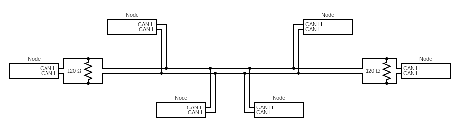
Automatic Bus Speed Detection
On powerup the device will scan the CAN bus and attempt to establish communication. If this is unsuccessful, it will cycle through a range of preset speeds until a connection is achieved. It will then store the successful speed and use it as it’s first attempt at next power up.
The cycled speed presets are: 1 Mbit/s, 500 Kbit/s, 250 Kbit/s, 125 Kbit/s.
This functionality can be disabled by the user if required.
Message Addressing
By default, the μPDM4’s CAN base address is 416 (0x1A0).
Tx frames are transmitted at a base address offset of 0 through 15 (416-431 by default).
Rx frames are accepted from base address offset 16 through 31 (432-447 by default).
The base address can be changed by the user, but it must be a multiple of 32 (0x20).
Caution
When more than one μPDM4 are on the same bus, their base address’s must be set independently and in multiples of at 32 (0x20).
Disconnect other devices which may be trying to use the same ID’s while you configure each device.
CAN Protocol Frames
Default Base ID: 416 (0x1A0)
Default Bitrate: Auto detect (Up to 1Mbit/s, FD Disabled, 11 bit Standard ID’s)
Tx Byte Order: MSB First (Unless specified otherwise)
Frame ID = Device Base ID + Frame Base ID Offset. For example: By default, Rx Frame 5 will be accepted on ID 437 (0x1B5).
Tx Data Stream
These frames are continually transmitted to the CAN bus. They contain lots of data about the device’s operational status.
Tx Frame 0: Device ID
Base ID Offset: 0 (0x00) | DLC: 8 | Rate: 1 Hz
| Data | Byte | Length (Bits) | Signed | Multiplier | Offset | Units | Decimals | Usage |
|---|---|---|---|---|---|---|---|---|
| Manufacturer ID | 0 | 8 | No | 1 | 0 | None | 0 | Always = 222 |
| Device Type ID | 1 | 8 | No | 1 | 0 | None | 0 | UPDM4 = 150 |
| Firmware Major | 2 | 8 | No | 1 | 0 | None | 0 | |
| Firmware Minor | 3 | 8 | No | 1 | 0 | None | 0 | |
| Firmware Revision | 4 | 8 | No | 1 | 0 | None | 0 | |
| Firmware Build | 5 | 16 | No | 1 | 0 | None | 0 | |
| Device Status | 7 | 8 | No | 1 | 0 | Status* | 0 |
* See Status Enumerations
Tx Frame 1: Time & Device Critical Stats
Base ID Offset: 1 (0x01) | DLC: 8 | Rate: 1 Hz
| Data | Byte | Length (Bits) | Signed | Multiplier | Offset | Units | Decimals | Usage |
|---|---|---|---|---|---|---|---|---|
| Uptime Days | 0 | 8 | No | 1 | 0 | Days | 0 | 12 = 12 Days |
| Uptime Hours | 1 | 8 | No | 1 | 0 | Hours | 0 | 12 = 12 Hours |
| Uptime Minutes | 2 | 8 | No | 1 | 0 | Minutes | 0 | 12 = 12 Minutes |
| Uptime Seconds | 3 | 8 | No | 1 | 0 | Seconds | 0 | 12 = 12 Seconds |
| CPU Temperature | 4 | 8 | No | 1 | -50 | °C | 0 | 123 = 73 °C |
| CPU Load | 5 | 8 | No | 1 | 0 | % | 0 | 12 = 12 % |
| Internal 5V0 Supply | 6 | 16 | No | 0.001 | 0 | Volts | 3 | 1234 = 1.234 Volts |
Tx Frame 2: Output Status & Load
Base ID Offset: 2 (0x02) | DLC: 8 | Rate: 10 Hz
| Data | Byte | Length (Bits) | Signed | Multiplier | Offset | Units | Decimals | Usage |
|---|---|---|---|---|---|---|---|---|
| Output 1 Status | 0 | 8 | No | 1 | 0 | Status* | 0 | |
| Output 2 Status | 1 | 8 | No | 1 | 0 | Status* | 0 | |
| Output 3 Status | 2 | 8 | No | 1 | 0 | Status* | 0 | |
| Output 4 Status | 3 | 8 | No | 1 | 0 | Status* | 0 | |
| Output 1 Load | 4 | 8 | No | 1 | 0 | % | 0 | 12 = 12% |
| Output 1 Load | 5 | 8 | No | 1 | 0 | % | 0 | |
| Output 1 Load | 6 | 8 | No | 1 | 0 | % | 0 | |
| Output 1 Load | 7 | 8 | No | 1 | 0 | % | 0 |
* See Status Enumerations
Tx Frame 3: Input Status
Base ID Offset: 3 (0x03) | DLC: 8 | Rate: 10 Hz
| Data | Byte | Length (Bits) | Signed | Multiplier | Offset | Units | Decimals | Usage |
|---|---|---|---|---|---|---|---|---|
| Input 1 Status | 0 | 8 | No | 1 | 0 | Status* | 0 | |
| Input 2 Status | 1 | 8 | No | 1 | 0 | Status* | 0 | |
| Input 3 Status | 2 | 8 | No | 1 | 0 | Status* | 0 | |
| Input 4 Status | 3 | 8 | No | 1 | 0 | Status* | 0 | |
| Input 5 Status | 4 | 8 | No | 1 | 0 | Status* | 0 | |
| Input 5 Volts | 5 | 16 | No | 0.001 | 0 | Volts | 3 | 12345 = 12.345 Volts |
| Input Level Flags | 7 | 8 | No | 1 | 0 | Bitfield** | 0 | See Input Level Bitfield |
* See Status Enumerations
** See Bitfield Enumerations
Tx Frame 4: Input Frequency
Base ID Offset: 4 (0x04) | DLC: 8 | Rate: 10 Hz
| Data | Byte | Length (Bits) | Signed | Multiplier | Offset | Units | Decimals | Usage |
|---|---|---|---|---|---|---|---|---|
| Input 1 Frequency | 0 | 16 | No | 0.1 | 0 | Hz | 1 | 1234 = 123.4 Hz |
| Input 2 Frequency | 1 | 16 | No | 0.1 | 0 | Hz | 1 | |
| Input 3 Frequency | 2 | 16 | No | 0.1 | 0 | Hz | 1 | |
| Input 4 Frequency | 3 | 16 | No | 0.1 | 0 | Hz | 1 |
Tx Frame 5: Device Totals Data
Base ID Offset: 5 (0x05) | DLC: 8 | Rate: 20 Hz
| Data | Byte | Length (Bits) | Signed | Multiplier | Offset | Units | Decimals | Usage |
|---|---|---|---|---|---|---|---|---|
| Battery Voltage | 0 | 16 | No | 0.001 | 0 | Volts | 3 | 12345 = 12.345 Volts |
| Total Current | 2 | 16 | No | 0.01 | 0 | Amps | 2 | 1234 = 12.34 Amps |
| Total Power | 4 | 16 | No | 0.1 | 0 | Watts | 1 | 1234 = 123.4 Watts |
| Total Load | 6 | 16 | No | 0.01 | 0 | % | 1 | 1234 = 12.34 % |
Tx Frame 6: Output Current Draw
Base ID Offset: 6 (0x06) | DLC: 8 | Rate: 20 Hz
| Data | Byte | Length (Bits) | Signed | Multiplier | Offset | Units | Decimals | Usage |
|---|---|---|---|---|---|---|---|---|
| Output 1 Current | 0 | 16 | No | 0.01 | 0 | Amps | 2 | 1234 = 12.34 Amps |
| Output 2 Current | 2 | 16 | No | 0.01 | 0 | Amps | 2 | |
| Output 3 Current | 4 | 16 | No | 0.01 | 0 | Amps | 2 | |
| Output 4 Current | 6 | 16 | No | 0.01 | 0 | Amps | 2 |
Tx Frame 7: Output Voltage
Base ID Offset: 7 (0x07) | DLC: 8 | Rate: 20 Hz
| Data | Byte | Length (Bits) | Signed | Multiplier | Offset | Units | Decimals | Usage |
|---|---|---|---|---|---|---|---|---|
| Output 1 Volts | 0 | 16 | No | 0.001 | 0 | Volts | 3 | 12345 = 12.345 Volts |
| Output 2 Volts | 2 | 16 | No | 0.001 | 0 | Volts | 3 | |
| Output 3 Volts | 4 | 16 | No | 0.001 | 0 | Volts | 3 | |
| Output 4 Volts | 6 | 16 | No | 0.001 | 0 | Volts | 3 |
Tx Frames 8-12: RESERVED
Rx Control Frames
Sending data to the device with these frames allows other devices to control the μPDM4’s behavior.
Rx Frame 0: Control Frame 1
Base ID Offset: 16 (0x10) | DLC: 8 | Timeout: 1.0 Seconds
| Data | Byte | Length (Bits) | Signed | Multiplier | Offset | Units | Decimals | Usage |
|---|---|---|---|---|---|---|---|---|
| Output 1 Duty Override | 0 | 8 | No | 1 | 1 or 100 | % DC | 0 | 0 = No Change |
| Output 2 Duty Override | 1 | 8 | No | 1 | 1 or 100 | % DC | 0 | 1 = Off (0 %DC) |
| Output 3 Duty Override | 2 | 8 | No | 1 | 1 or 100 | % DC | 0 | 2 = On (100 %DC) |
| Output 4 Duty Override | 3 | 8 | No | 1 | 1 or 100 | % DC | 0 | 100 - 200 = 0 - 100 %DC |
| Output 1 & 2 Frequency Override | 4 | 8 | No | 1 | 0 | Hz | 0 | 0 = No Change |
| Output 1 & 2 Frequency Override | 5 | 8 | No | 1 | 0 | Hz | 0 | 1 - 200 = 1 - 200 Hz |
| Output 3 & 4 Frequency Override | 6 | 8 | No | 1 | 0 | Hz | 0 | |
| Output 3 & 4 Frequency Override | 7 | 8 | No | 1 | 0 | Hz | 0 |
Rx Frame 1: Control Frame 2
Base ID Offset: 17 (0x11) | DLC: 8 | Timeout: 3.0 Seconds
| Data | Byte | Length (Bits) | Signed | Multiplier | Offset | Units | Decimals | Usage |
|---|---|---|---|---|---|---|---|---|
| Output 1 Fuse Current Override | 0 | 8 | No | 0.1 | 0 | Amps | 1 | 0 = No Change |
| Output 2 Fuse Current Override | 1 | 8 | No | 0.1 | 0 | Amps | 1 | 123 = 12.3 Amps |
| Output 3 Fuse Current Override | 2 | 8 | No | 0.1 | 0 | Amps | 1 | |
| Output 4 Fuse Current Override | 3 | 8 | No | 0.1 | 0 | Amps | 1 | |
| Output 1 Retries Override | 4 | 8 | No | 1 | 1 | None | 0 | 0 = No Change |
| Output 2 Retries Override | 5 | 8 | No | 1 | 1 | None | 0 | 1 - 254 = 0 - 253 Retires |
| Output 2 Retries Override | 6 | 8 | No | 1 | 1 | None | 0 | 255 = Always Retry |
| Output 4 Retries Override | 7 | 8 | No | 1 | 1 | None | 0 |
Rx Frame 2: Control Frame 3 (Emtron Friendly)
Base ID Offset: 18 (0x12) | DLC: 8 | Timeout: 3.0 Seconds
| Data | Byte | Length (Bits) | Signed | Multiplier | Offset | Units | Decimals | Usage |
|---|---|---|---|---|---|---|---|---|
| Output 1 Enable Override | 0 | 16 (LSB First) | No | 1 | 0 | None | 0 | 0 = No Change |
| Output 1 Enable Override | 2 | 16 (LSB First) | No | 1 | 0 | None | 0 | 1 = On (100% DC) |
| Output 1 Enable Override | 4 | 16 (LSB First) | No | 1 | 0 | None | 0 | |
| Output 1 Enable Override | 6 | 16 (LSB First) | No | 1 | 0 | None | 0 |
Rx Frames 3-12: RESERVED
Device Config Frames
These frames allow the reading & writing of internal configuration data. They are mostly for use by configuration & tuning interfaces such as MectriCal & MectriCAN though any device capable of sending a single CAN frame can use them.
See Simplified CAN Programming for usage of the Special Command Frame
Rx Frame 13: Special Command
Base ID Offset: 29 (0x1D) | DLC: 8
| Data | Byte | Length (Bits) | Signed | Multiplier | Offset | Units | Decimals | Usage |
|---|---|---|---|---|---|---|---|---|
| Command ID | 0 | 8 | No | 1 | 0 | None | 0 | See Commands Table |
| Data 0 | 1 | ** | ** | ** | ** | ** | ** | |
| Data 1 | 2 | ** | ** | ** | ** | ** | ** | |
| Data 2 | 3 | ** | ** | ** | ** | ** | ** | |
| Data 3 | 4 | ** | ** | ** | ** | ** | ** | |
| Data 4 | 5 | ** | ** | ** | ** | ** | ** | |
| Checksum (where applicable) | 6 | 16 (LSB First) | No | 1 | 0 | None | 0 | Sum (Bytes 0:5) + 1 |
The device will respond via Tx Frame 13.
Tx Frame 13: Special Command Response
Base ID Offset: 13 (0x0D) | DLC: 8 | Rate: Once
| Data | Byte | Length (Bits) | Signed | Multiplier | Offset | Units | Decimals | Usage |
|---|---|---|---|---|---|---|---|---|
| Command ID | 0 | 8 | No | 1 | 0 | None | 0 | See Commands Table |
| Data 0 | 1 | ** | ** | ** | ** | ** | ** | |
| Data 1 | 2 | ** | ** | ** | ** | ** | ** | |
| Data 2 | 3 | ** | ** | ** | ** | ** | ** | |
| Data 3 | 4 | ** | ** | ** | ** | ** | ** | |
| Data 4 | 5 | ** | ** | ** | ** | ** | ** | |
| Checksum (where applicable) | 6 | 16 (LSB First) | No | 1 | 0 | None | 0 | Sum (Bytes 0:5) + 1 |
Rx Frame 14: Configuration Read Request
Base ID Offset: 40 (0x1E) | DLC: 3
| Data | Byte | Length (Bits) | Signed | Multiplier | Offset | Units | Decimals | Usage |
|---|---|---|---|---|---|---|---|---|
| Config Variable Type | 0 | 8 | No | 1 | 0 | None | 0 | |
| Config Variable ID | 1 | 16 (LSB First) | No | 1 | 0 | None | 0 |
The device will respond via Tx Frame 14.
Tx Frame 14: Configuration Read Response
Base ID Offset: 14 (0x0E) | DLC: 8 | Rate: Once
| Data | Byte | Length (Bits) | Signed | Multiplier | Offset | Units | Decimals | Usage |
|---|---|---|---|---|---|---|---|---|
| Read Item Type | 0 | 8 | No | 1 | 0 | None | 0 | 255 = Invalid Request |
| Read Item ID | 1 | 16 (LSB First) | No | 1 | 0 | ID | 0 | > 65500 = Error |
| Data 0 | 3 | 8 | ** | ** | ** | ** | ** | LSB First |
| Data 1 | 4 | 8 | ** | ** | ** | ** | ** | |
| Data 2 | 5 | 8 | ** | ** | ** | ** | ** | |
| Data 3 | 6 | 8 | ** | ** | ** | ** | ** | |
| Data 4 | 7 | 8 | ** | ** | ** | ** | ** |
Rx Frame 15: Configuration Write Command
Base ID Offset: 31 (0x1F) | DLC: 8
| Data | Byte | Length (Bits) | Signed | Multiplier | Offset | Units | Decimals | Usage |
|---|---|---|---|---|---|---|---|---|
| Config Variable Type | 0 | 8 | No | 1 | 0 | None | 0 | |
| Config Variable ID | 1 | 16 (LSB First) | No | 1 | 0 | None | 0 | |
| Config New Value | 3 | 32(LSB First) | ** | ** | ** | ** | ** | |
| Store All Changes | 7 | 8 | No | 1 | 0 | None | 0 | 0 = No, 1 = Store All |
The device will respond via Tx Frame 15.
Tx Frame 15: Configuration Write Response
Base ID Offset: 15 (0x0F) | DLC: 8 | Rate: Once
| Data | Byte | Length (Bits) | Signed | Multiplier | Offset | Units | Decimals | Usage |
|---|---|---|---|---|---|---|---|---|
| Config Variable Type | 0 | 8 | No | 1 | 0 | None | 0 | 255 = Wrong Variable Type |
| Config Variable ID | 1 | 16 (LSB First) | No | 1 | 0 | ID | 0 | > 65500 = Error |
| Config New Value | 3 | 32(LSB First) | ** | ** | ** | ** | ** | New value of the variable |
| Store All Changes | 7 | 8 | No | 1 | 0 | None | 0 | 0 = No, 1 = Store Complete |
Simplified CAN Programming
In the absence of a MectriCAN interface, basic config changes can be made by any device capable of sending a CAN message. The following protocol is provided to simplify this process.
Configuration changes are written using Rx Frame 13 (ID + 29) and responses will be transmitted on Tx Frame 13 (ID + 13). For simplicity the requirement for a checksum has been omitted for these commands. Frames must be 8 bytes long or they will be ignored. Unused bytes can contain 0’s.
Command ID is placed in Byte 0. Data is placed in Bytes 1-7 as required. If the configuration sent differs from the current data in memory, the response frame will contain a value of 1 in Byte 1. This means the new configuration has been changed and stored in permanent memory. If the same frame is sent again without new configuration changes, response Byte 1 will be 0.
Commands
| ID | Command |
|---|---|
| 10 | Output Current Limits |
| 11 | Output Retries |
| 12 | Output Retry Delays |
| 13 | Output Soft Start Initial Duty Cycles |
| 14 | Output Soft Start Times |
| 15 | Output Max Duty Cycles |
| 16 | Output Frequencies |
| 20 | Input Pin Config |
| 21 | Switch Active Levels |
| 30 | Logic Conditions |
| 31 | CAN Config |
Response Frame
The response frame will contain the following data:
Byte 0: Command ID (255 = Error).
Byte 1: 0 = No change to current config (data sent matches data stored), 1 = Change made and stored in memory.
Byte 2-7: Not used, will contain all 0’s.
| ID | DLC | Byte 0 | Byte 1 | Byte 2 | Byte 3 | Byte 4 | Byte 5 | Byte 6 | Byte 7 |
|---|---|---|---|---|---|---|---|---|---|
| BASE + 13 | 8 | Command ID | O or 1 | 0 | 0 | 0 | 0 | 0 | 0 |
Output Current Limits
Sets the current limit for the outputs.
Command ID: 10
Data Units: Amps
Data Multiplier: 0.1
Data Usage: (123 = 1.23 Amps)
| ID | DLC | Byte 0 | Byte 1 | Byte 2 | Byte 3 | Byte 4 | Byte 5 | Byte 6 | Byte 7 |
|---|---|---|---|---|---|---|---|---|---|
| BASE + 29 | 8 | 10 | Output 1 Max Current | Output 2 Max Current | Output 3 Max Current | Output 4 Max Current | 0 | 0 | 0 |
Output Retries
Sets the maximum number of times each output will be retried after a fault is detected.
Command ID: 11
Data Units: None
Data Multiplier: 1
Data Usage: 0-254 = 0-254 Retries, 255 = Always Retry.
| ID | DLC | Byte 0 | Byte 1 | Byte 2 | Byte 3 | Byte 4 | Byte 5 | Byte 6 | Byte 7 |
|---|---|---|---|---|---|---|---|---|---|
| BASE + 29 | 8 | 11 | Output 1 Max Retries | Output 2 Max Retries | Output 3 Max Retries | Output 4 Max Retries | 0 | 0 | 0 |
Output Retry Delay
Sets the amount of time that the output must remain off after a fault is cleared before it will be retried.
Command ID: 12
Data Units: Seconds
Data Multiplier: 0.1
Data Usage: 123 = 12.3 Seconds
| ID | DLC | Byte 0 | Byte 1 | Byte 2 | Byte 3 | Byte 4 | Byte 5 | Byte 6 | Byte 7 |
|---|---|---|---|---|---|---|---|---|---|
| BASE + 29 | 8 | 12 | Output 1 Retry Delay | Output 2 Retry Delay | Output 3 Retry Delay | Output 4 Retry Delay | 0 | 0 | 0 |
Output Soft Start Initial Duty Cycle
Sets the initial duty cycle used when an output’s Soft Start Time > 0.
Command ID: 13
Data Units: %DC
Data Multiplier: 1
Data Usage: 12 = 12 %DC
| ID | DLC | Byte 0 | Byte 1 | Byte 2 | Byte 3 | Byte 4 | Byte 5 | Byte 6 | Byte 7 |
|---|---|---|---|---|---|---|---|---|---|
| BASE + 29 | 8 | 13 | Output 1 Start Duty | Output 2 Start Duty | Output 3 Start Duty | Output 4 Start Duty | 0 | 0 | 0 |
Output Soft Start Time
Sets the amount of time taken to ramp from the output’s Initial Duty Cycle value to the output’s Maximum Duty value.
Command ID: 14
Data Units: Seconds
Data Multiplier: 0.1
Data Usage: 123 = 12.3 Seconds
| ID | DLC | Byte 0 | Byte 1 | Byte 2 | Byte 3 | Byte 4 | Byte 5 | Byte 6 | Byte 7 |
|---|---|---|---|---|---|---|---|---|---|
| BASE + 29 | 8 | 14 | Output 1 Start Time | Output 2 Start Time | Output 3 Start Time | Output 4 Start Time | 0 | 0 | 0 |
Output Max Duty Cycle
Sets the maximum duty cycle for the output. Be careful when using values less then 100% as external flywheel diodes may be required. See DC Motors.
Command ID: 15
Data Units: %DC
Data Multiplier: 1
Data Usage: 12 = 12 %DC
| ID | DLC | Byte 0 | Byte 1 | Byte 2 | Byte 3 | Byte 4 | Byte 5 | Byte 6 | Byte 7 |
|---|---|---|---|---|---|---|---|---|---|
| BASE + 29 | 8 | 15 | Output 1 Max Duty | Output 2 Max Duty | Output 3 Max Duty | Output 4 Max Duty | 0 | 0 | 0 |
Output Frequency
Sets the frequency used by the outputs during Soft Start or similar PWM mode.
Command ID: 16
Data Units: Hz
Data Multiplier: 1
Data Usage: 123 = 123 Hz (200 Hz Max)
| ID | DLC | Byte 0 | Byte 1 | Byte 2 | Byte 3 | Byte 4 | Byte 5 | Byte 6 | Byte 7 |
|---|---|---|---|---|---|---|---|---|---|
| BASE + 29 | 8 | 16 | Output 1 Frequency | Output 2 Frequency | Output 3 Frequency | Output 4 Frequency | 0 | 0 | 0 |
Input Pin Config
Sets the active level and edge of the input pin.
Command ID: 20
Data Units: Bitfield
Data Multiplier: 1
Data Usage:
- Bit 0 = Active Level (0 = Low, 1 = High)
- Bit 1:5 = Not Used
- Bit 6:7 = Active Edge (0 = Low, 1 = High, 2 = Both)
| ID | DLC | Byte 0 | Byte 1 | Byte 2 | Byte 3 | Byte 4 | Byte 5 | Byte 6 | Byte 7 |
|---|---|---|---|---|---|---|---|---|---|
| BASE + 29 | 8 | 20 | Input 1 Config | Input 2 Config | Input 3 Config | Input 4 Config | 0 | 0 | 0 |
Input Switch Active Level
Sets the active level of the Input Switch functions. By default, these values represent Input Pin levels for the switches to be considered ON. Byte 6 contains a bitfield that sets the Switches toggle/latch functionality.
Command ID: 21
Data Units: None
Data Multiplier: 1
Data Usage:
- Switch Active Level: 0 = Low, 1 = High.
- Switch Toggle Flags: Bit 0:5 = Switch 1-5 Toggle/Latch (0 = Off, 1 = On).
| ID | DLC | Byte 0 | Byte 1 | Byte 2 | Byte 3 | Byte 4 | Byte 5 | Byte 6 | Byte 7 |
|---|---|---|---|---|---|---|---|---|---|
| BASE + 29 | 8 | 21 | Switch 1 Active Level | Switch 2 Active Level | Switch 3 Active Level | Switch 4 Active Level | Switch 5 Active Level | Switch Toggle Flags | 0 |
Logic Conditions
Sets the requirements for the output switch logic. This is an extremely simplified implementation of the internal logic.
Command ID: 30
Data Units: None
Data Multiplier: 1
Data Usage:
- 0 = Output# will turn on if: Switch# = ON.
- 1 = Output# will turn on if: Switch# = ON AND Switch5 = ON.
- 2 = Output# will turn on if: Switch# = ON AND Switch1 = ON.
- 3 = Output# will turn on if: Switch# = ON AND (Switch5 = ON OR Switch1 = ON). This is the default configuration.
| ID | DLC | Byte 0 | Byte 1 | Byte 2 | Byte 3 | Byte 4 | Byte 5 | Byte 6 | Byte 7 |
|---|---|---|---|---|---|---|---|---|---|
| BASE + 29 | 8 | 30 | Logic 1 Mode | Logic 2 Mode | Logic 3 Mode | Logic 4 Mode | 0 | 0 | 0 |
CAN Configuration
Sets the CAN Base Address, Bitrate, and Auto Speed Detection.
Changes will take effect after a full power cycle.
Command ID: 31
Data Units: None
Data Multiplier: 1
Data Usage:
- Base Address (Bytes 1:4): 32-bit unsigned integer, LSB First, internally masked to multiples of 32.
- Bitrate Mode (Byte 5): 1 = 125 Kbit/s, 2 = 250 Kbit/s, 3 = 500 Kbit/s, 4 = 1 Mbit/s.
- Auto Speed Detection (Byte 6): 0 = Off, 1 = On.
| ID | DLC | Byte 0 | Byte 1 | Byte 2 | Byte 3 | Byte 4 | Byte 5 | Byte 6 | Byte 7 |
|---|---|---|---|---|---|---|---|---|---|
| BASE + 29 | 8 | 31 | Base Address [0] | Base Address [1] | Base Address [2] | Base Address [3] | Bitrate Mode | Auto Speed Detection | 0 |
Data Enumerations
Device Status
| Value | Status | Description |
|---|---|---|
| 1 | OK | The output channel is on and OK. |
| 5 | Over Current | The device’s total maximum current draw fault has been triggered. |
| 6 | Over Voltage | The device’s supply voltage has exceeded 18.0 Volts. |
| 7 | Overload | The device’s total maximum load fault has been triggered. |
| 8 | Short Circuit or Over Temp | All output channel’s driver IC’s have detected either a short circuit or over heated. |
| 10 | Retry Limit | The device’s retry limit has been reached. All outputs are Off. |
Output Status
| Value | Status | Description |
|---|---|---|
| 0 | Off | The output channel is switched off. |
| 1 | On | The output channel is on and OK. |
| 2 | RESERVED | - |
| 3 | Soft Start | Soft start is currently active on the output channel. |
| 4 | Override Active | The output is being commanded by a configuration override variable. |
| 5 | Over Current | The output channel’s maximum current draw fault has been triggered. |
| 6 | Over Voltage | The output channel’s voltage has exceeded 18.0 Volts. |
| 7 | Overload | The output channel’s maximum load fault has been triggered. |
| 8 | Short Circuit or Over Temp | The output channel’s driver IC has detected either a short circuit or over heated. |
| 9 | Open Circuit | The output channel is on but there is no current draw. |
| 10 | Retry Limit | The output channel’s retry limit has been reached. The output is Off. |
Input Status
| Value | Status | Description |
|---|---|---|
| 0 | Off / Inactive | The input channel’s voltage level IS NOT equal to its active level. |
| 1 | On / Active | The input channel’s voltage level IS equal to its active level. |
| 2 | PWM Signal Lost | The input channel has transitioned from a PWM input to a static signal. |
| 3 | PWM Signal Active | The input channel is measuring an incoming waveform. |
Input Level Bitfield
| Bit | Input | Description |
|---|---|---|
| 0 | IN1 | 0 = Low, 1 = High |
| 1 | IN2 | 0 = Low, 1 = High |
| 2 | IN3 | 0 = Low, 1 = High |
| 3 | IN4 | 0 = Low, 1 = High |
| 4 | IN5 | 0 = Low, 1 = High |
Inputs Pins
Input pins (INn) can be used as switch inputs or waveform inputs. Inputs 1-5 have Schmitt trigger circuits and will transition from a low to a high state with a small amount of hysteresis. The inputs are compatible with VR sensor AC waves as long as the voltage levels are high enough to trigger the input thresholds.
Each input can measure the frequency, duty cycle, and pulse width of an input waveform up to 500Hz. These values can be used by any function and/or directed straight to control an output pin(s).
Voltage Measurement
Inputs can measure input voltage of 0-20V. This can be used by any logic function.
On Rev 1 hardware (Serial# < 2000), voltage measurement is only available on IN5.
Digital Thresholds
High Input Threshold: ~2.7 Volts.
Low Input Threshold: ~2.0 Volts.
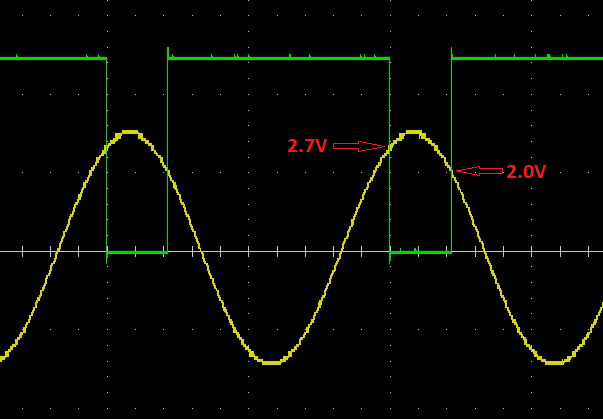
Input Schmitt Trigger with a +- 3.0V AC waveform input (Yellow). Note the Green trace represents the output of the Schmitt trigger circuit which is inverse to the actual waveform input. The result is inverted by software to represent the true input level.
Input Pullups
All input pins have configurable 4K7 pullups to 5V. When enabled, unloaded input pin voltage will sit at approximately 3.6V.
Configruable pullups are not available on Rev 1 hardware (Serial# < 2000).
Output Pins
Output Pins (OUTn) can supply external loads with a controlled and protected source voltage. Each output is protected against overload, short circuit, over voltage, and over temperature. Fuse current’s can be configured along with retry delays and limits.
Each output driver is rated to capable of 15A continuous load, more in short burst and inrush conditions.
PWM
Each output can be PWM’d at up to 200Hz, allowing current/speed control of load devices such as globes, pumps, and fans.
Warning
Care must be taken when PWM controlling highly inductive loads and external flywheel diodes must be fitted. See the section on DC Motors for details.
Rev 2 Hardware: Frequencies are shared between OUT3 & OUT4.
Rev 1 Hardware: Frequencies are shared between OUT1 & OUT2 as well as between OUT3 & OUT4.
In the case of shared frequency outputs, the OUTn channel requesting the lowest frequency will gain control. Care should be taken to choose appropriate channels for certain tasks.
For example:
- OUT1 = Left indicator lamps @ 1Hz.
- OUT2 = Right Indicator lamps @ 1Hz.
- OUT3 = Fuel pump @ 100 Hz.
- OUT4 = Thermo Fan @ 100 Hz.
If you were to try to run OUT3 at 100Hz and OUT4 at 200 Hz, both channels will operate at 100Hz.
Device Current Limit
The device maximum current limitation is 65A.
If the current draw exceeds this value for more than 5 seconds, the device total current limit fault will be triggered, and all outputs will turn off.
Short Circuit Protection
In the event of a short circuit between a OUTn channel and GND, a very high current will flow through the device. This current will exceed the output’s hardware over current threshold and the OUTn channel will be switched off.
Over Temp Protection
Any output channel (OUTn) supplying an excessive current load will cause the output driver to heat up. In the event of excessive IC temperature, OUTn will switch OFF. The output will remain off for the duration of the configured Retry Delay time. If the channel’s configured Retry Limit has not been reached, the output will switch back on.
Reverse Battery Protection
Battery voltage is distributed to the µPDM4’s internal circuitry through an array of high current P-Channel MOSFETs. These will block the flow of reverse current to the device itself as well as any load it is supplying.
Over Load Protection
Each output channel (OUTn) calculates a Load value represented in percent. Load is a function of accumulated current draw over time compared to the output’s configured Fuse Current. If the Load figure reaches 100% for more that the output’s configured Fault Delay time, OUTn will switch OFF. The output will remain off for the duration of the configured Retry Delay time. If the channel’s configured Retry Limit has not been reached, the output will switch back on.
Over Current Protection
Each output channel (OUTn) measures a live current draw value represented in amps. If the current draw exceeds the configured Fuse Current by more than 2.0A for more longer than the output’s configured Fault Delay time, OUTn will switch OFF. The output will remain off for the duration of the configured Retry Delay time. If the channel’s configured Retry Limit has not been reached, the output will switch back on.
Soft Start
Outputs can be enabled to utilize a Soft Start function. When the configured OUTn Soft Start Time is non 0, the output will ramp up from its Start Duty value to its final duty cycle over the specified time period. This helps to reduce the inrush current of high draw loads and reduce effects like headlights dimming when fans turn on.
DC Motors (Fans, Pumps, etc.)
When driving high current inductive loads such as thermo fans and pumps it’s recommended to install a large external flywheel diode across the motor terminals. This is particularly important if the motor is to be speed controlled by PWM.
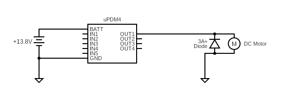
Required external flywheel diode for DC motor PWM operation.
When the output switches off, the motor will induce a large negative voltage that the driver IC must try and dissipate. During PWM operation, this happens up to 200 times per second, causing excessive heat to build up in the IC. A diode rated for at least 3A and 50V should suffice. The test below was done with a 1N5404.
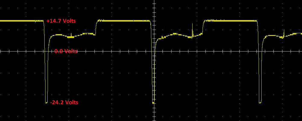
100Hz, 50% Duty PWM, no diode fitted. Output channel voltage is subjected to a large negative voltage when the IC switches off.
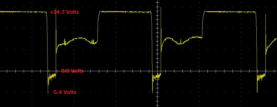
100Hz, 50% Duty, Diode Installed. The negative voltage spike is largely absorbed.
Device Ratings
| Parameter | Value |
|---|---|
| Processor | 48 MHz, 32 Bit, Cortex M0 |
| CAN | 1x 2.0A/2.0B/FD |
| Inputs | 5x Analogue/Digital |
| Outputs | 4x High Side |
| Minimum operating voltage | 6.0 V |
| Minimum operating voltage (cranking) | 6.0 V |
| Maximum operating voltage | 27 V (Software limited to 18 V) |
| Maximum current draw in OFF state (all outputs OFF, CPU & CAN active) | 21 mA |
| Input LOW threshold | ~2.0 V |
| Input HIGH threshold | ~3.0 V |
| Output typical ON-state resistance (TJ = 25 °C) | 2.5 mΩ |
| Output maximum ON-state resistance (TJ = 150 °C) | 5 mΩ |
| Output IC nominal rated load current (TA = 85 °C) | 24 A |
| Output IC minimum overload detection current | 65 A |
| Device total current limit | 65 A |
| Minimum operating temperature | -40 °C |
| Maximum operating temperature | 105 °C |
| Minimum component automotive qualification | AEC-Q100 Grade 2 |
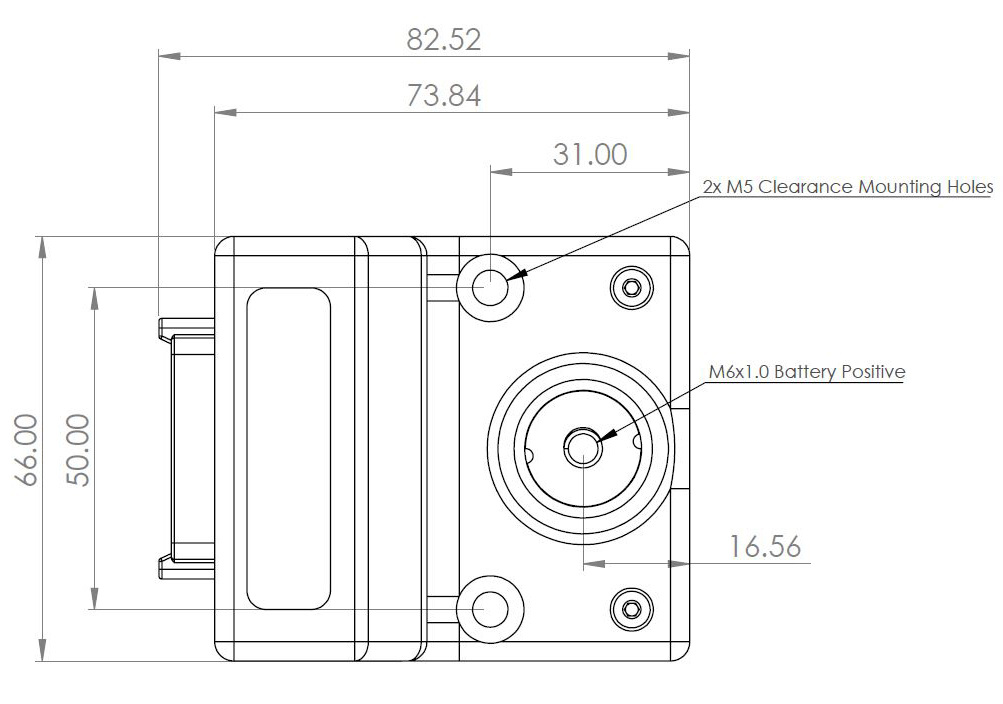
Dimensions